Applied Materials、次世代OLED製造用の新たなアーキテクチャとツールを発表~Samsung Displayが評価中
関連調査レポート Quarterly Display Capex and Equipment Market Share Report の詳細仕様・販売価格・一部実データ付き商品サンプル・WEB無料ご試読は こちらから お問い合わせください。
これらDSCC Japan発の分析記事をいち早く無料配信するメールマガジンにぜひご登録ください。ご登録者様ならではの優先特典もご用意しています。【簡単ご登録は こちらから 】
記事のポイント
- Applied Materials (AMAT) は次世代OLED製造用の新たなアーキテクチャとツールの開発に以前から取り組んできた。OLEDメーカーのJapan DisplayとVisionoxも同技術を推進しており、生産に近づいている。
- AMATが今回発表した新たなソリューションはMAX OLEDと呼ばれるもので、市場リーダーであるSamsung Displayが同技術を評価するためアルファシステムに導入することも発表した。
- AMATが成功すればOLEDフロントプレーン設備投資の生産ライン当たりの機会は10倍以上に拡大すると見られ、同社がFPD設備投資を独占する可能性がある。
Applied Materials Announces New Tool and Architecture for Next Generation OLED Manufacturing, Samsung Display Now Assessing Their Technology
- Applied Materials (AMAT) has been working on a new architecture and tool for manufacturing next generation OLEDs for some time. OLED manufacturers Japan Display and Visionox have been touting this technology and are nearing production.
- Applied has now gone public with their new solution which is called MAX OLED and they also announced that market leader Samsung Display is bringing in an alpha system to assess the technology.
- If successful, Applied is likely to dominate display equipment spending with their OLED frontplane equipment opportunity growing by more than 10X per fab according to our estimates.
OLEDs found in smartphones, tablets, laptops, smartwatches and automotive applications are fabricated using a fine metal mask vacuum thermal evaporation (FMM VTE) tool. While Applied hasn’t disclosed pricing for their solution, FMM VTE tools can cost $500M each at G8.7 for 7.5K capacity for a tandem stack and the total FMM VTE expenditure for a 15K substrate per month tandem OLED fab can reach $1B. Equipment suppliers can only make and install a couple of these giant tools per year which can easily fill a football field, constraining the pace at which OLED manufacturers can build and expand capacity targeting future applications. In addition, the FMMs constrain OLED performance and limit the maximum size that can be produced. The ultra-thin fine metal masks are inherently constrained by sag, geometrical distortion and the tapered hole shape which results in a smaller OLED pixel and aperture ratio than if they were patterned by lithography. As the FMMs grow, the problem gets worse. With panel manufacturers looking to use larger substrates and build larger panels, FMMs can compromise this effort. In addition, the FMMs themselves are also expensive, take a long time to manufacture, need to be cleaned regularly, can lead to cross contamination impacting yields and require very precise positioning which impacts tool costs and can impact yields.
What if there was a better way?
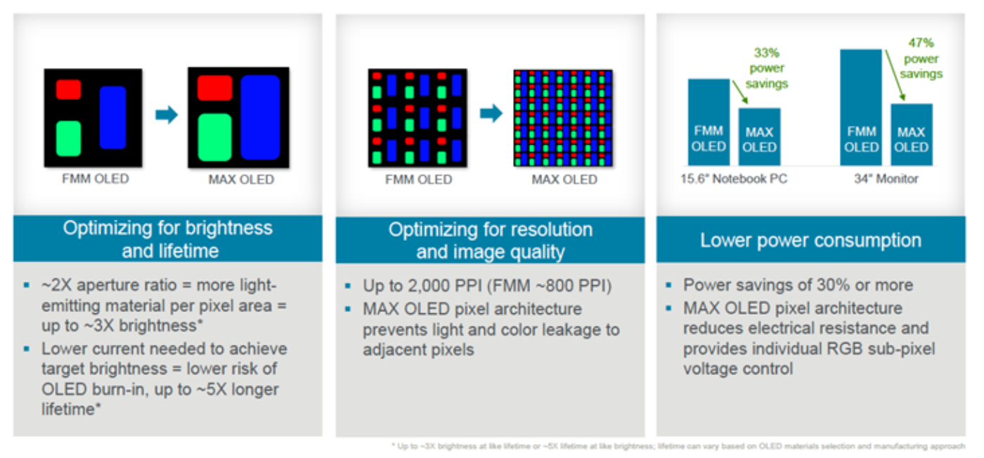
This is where Applied Materials comes in. They have developed an alternative approach which they call MAX OLED that does away with FMMs and FMM VTE tools. In addition, their approach can dramatically improve OLED performance, doubling the OLED pixel aperture ratio which can boost brightness by up to 3X and lifetime by up to 5X while reducing power consumption by more than 30% as shown in the figure below. Their approach can also increase resolution up to 2000 PPI, enabling OLEDs made on glass with this technology to cost effectively target the AR/VR market which currently can only be effectively addressed with more costly OLED on silicon or microLED technology. You may have heard about some or all of these claims before from Japan Display with their eLEAP technology and Visionox with their ViP technology, but both of these companies are relying on Applied’s MAX OLED tool and device architecture.
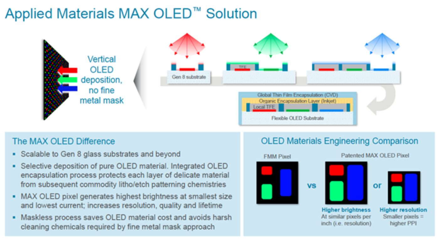
So, what is MAX OLED? Rather than evaporating the OLED materials upwards through the FMM in a large footprint FMM VTE system with panel suppliers requiring a smaller pixel aperture ratio to account for the additional margins required by the imprecise FMM and then encapsulating the OLED stack after all three colors have been formed, MAX OLED takes a different approach. MAX OLED evaporates each color in a separate smaller footprint, vertical mask-less evaporation tool that evaporates a blanket deposition of a single color and then encapsulates that color before it leaves the combination evaporation and thin film encapsulation (TFE) system. After each color is encapsulated, it is then patterned using photolithography resulting in a larger pixel aperture ratio due to the additional precision provided by the lithography process. The added precision from the photolithography process not only expands the aperture ratio but can also reduce crosstalk and improve yield in tandem stack devices. After the first color is patterned, then the second color is evaporated, encapsulated and patterned followed by the third color. After the full stack is evaporated and patterned, the conventional encapsulation process then takes place to protect the entire stack.
For Applied Materials, this is a huge opportunity to dominate the evaporation market which is expected to be the largest display equipment segment from 2025. In addition, it will significantly expand the encapsulation market where they are also dominant. In DSCC’s Quarterly Display Capex and Equipment Market Share Report, we show their frontplane equipment opportunity for a 15K G8.7 fab growing over 10X to over $750M. Furthermore, the device structure is patented and unique and Applied should be able to protect its IP if companies try to violate it. In fact, the patented device architecture which features an isolating pillar network structure, also helps to reduce crosstalk and color shift which boosts yields and can serve as an auxiliary electrode which can significantly reduce power.
While Visionox and JDI are expected to be the first companies to commercialize the MAX OLED technology, a partnership with market leader Samsung Display, who was the first company to enjoy commercial success with FMM technology and continues to enjoy the highest market share in RGB OLEDs, is very telling and important. SDC has the financial muscle to expand capacity faster than its competitors and achieve the full potential of MAX OLED technology, scaling it from 1” for AR/VR to any OLED TV size in a single fab if it chooses to do so. The MAX OLED technology has the potential to enable OLED manufacturers to target all applications from a single fab for the first time with the best performance and quality, ensuring maximum utilization. OLED manufacturers have not had this luxury to date, focusing on one or two applications per fab so far and subject to seasonal fluctuations in demand. We could see a burst in display industry capex once this technology is mastered and successful in mass production, enabling better performing OLED displays to take more share across a wide array of applications. In addition to the better performance, costs should be lower due to lower capex, elimination of FMM-related costs and higher material utilization.
According to Dr. Brian Shieh, Applied Materials Group Vice President and General Manager of their Display and Flexible Technology Business, “The consumer electronics business has been waiting for a breakthrough that can bring OLED technology to the hundreds of millions of tablets, PCs and TVs sold each year.” Applied believes it has delivered this breakthrough, and they are well positioned to monetize it and dominate future display equipment spending.


