Samsung DisplayがOrthogonalの特許の一部を金額非公開で取得~eLEAPやViPとの違いは?
これらDSCC Japan発の分析記事をいち早く無料配信するメールマガジンにぜひご登録ください。ご登録者様ならではの優先特典もご用意しています。【簡単ご登録は こちらから 】
冒頭部和訳
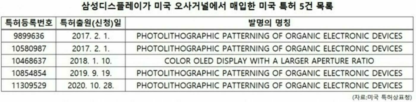
Samsung Displayが米国の新興企業OrthogonalのFMMレスOLED製造に関する特許のうち5件 (下図) を取得したことを The Elec が報じている。Orthogonalのアプローチは、Japan Display、Visionox、Applied Materialsの各社がこれまでに採用してきたアプローチとは異なる。決定的な違いは、OLED材料が成膜されてからOLEDスタックの後半部分が成膜されるまでの保護方法である。
Samsung Display Acquires Some of Orthogonal’s Patents for Undisclosed Sum, How It Differs with eLEAP and ViP
※ご参考※ 無料翻訳ツール (Google)The Elec reported that Samsung Display has acquired five of US start-up Orthogonal’s patents, shown below, for FMM-less OLED manufacturing. The approach Orthogonal took is different than the approach that Japan Display, Visionox and Applied Materials have taken. The key difference is how the OLED material is protected once it is deposited and when the second half of the OLED stack is deposited.
Orthogonal Patents Acquired by SDC
In both cases, the HIL/HTL and emitter layers are deposited by evaporation after the PDL is formed. However, the Orthogonal approach doesn’t evaporate the second half of the stack – EIL/ETL/cathode – until all three colors are patterned. On the other hand, the eLEAP/ViP approach evaporates the entire OLED stack for each color before patterning. In addition, in the Orthogonal case, their patents call for the slot coating of a fluorinated protection layer slot coat to protect the OLED layers before coating an “orthogonal” photoresist layer, then using lithography to pattern the underlying OLED layers. Once the device is completed, they evaporate the ETL/EIL/cathode layers and then encapsulate. So, there is just a single encapsulation step as in traditional RGB OLEDs, but three additional coating steps of this fluorinated protection layer, which is designed to prevent the photoresist, oxygen, water, etc. from damaging the underlying OLED layers.
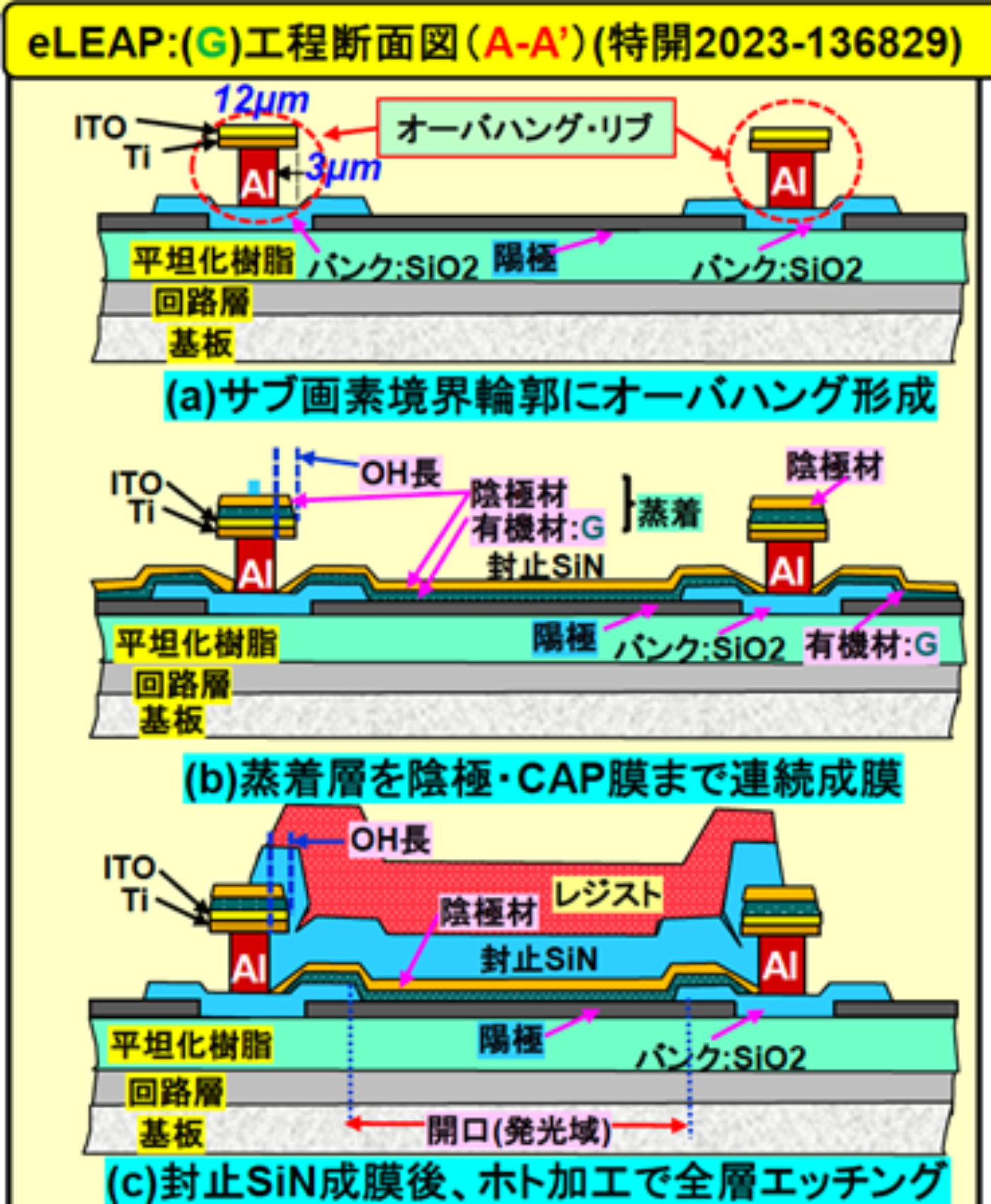
In the eLEAP/ViP case, the manufacturers are encapsulating the OLED layers with CVD TFE for each color and then patterning the underlying OLED layers. So, they replaced the Orthogonal’s fluorinated protection layer with CVD TFE. They have also incorporated a unique rib structure that ensures the encapsulation layers are separated by color and do not cause growing dark spots, see my Visionox write-up this issue. On this topic, at our April Japan Seminar, well known display technologist Kikuo One presented on the eLEAP structure which you can see below from their patent filings. You can also see the unique rib structure used to prevent growing dark spots among other functions.
JDI eLEAP Structure
The Orthogonal patents refer to a lift-off structure where the top portion is wider than the base portion. They also refer to a fluoropolymer coating step where the fluoropolymer is treated in a processing agent comprising a fluorinated solvent in which the fluoropolymer is soluble to form a processed intermediate structure. It is preferred that at least the layer or portion of the photoresist structure in contact with the OLED materials are a fluorinated polymer or molecular solid provided from a fluorinated coating solvent. In addition, they claim the use of “orthogonal” photoresist structures and processing agents that are compatible with sensitive organic electronic devices and materials. The photoresists are chosen to have low interaction with sensitive device layers that are not intended to be dissolved or otherwise damaged. Conventional photoresist materials use harsh organic solvents and often strongly caustic developers that can easily damage one or more layers of an OLED device.
If Orthogonal’s fluorinated protection layer worked effectively, it would result in lower capex and product costs due to fewer encapsulation steps. Although they reportedly developed at least a three-color passive matrix prototype with this technology, we never saw any demo’s and they pivoted to organic photodetectors for fingerprint sensing and licensing. It was rumored by one insider that there was damage to the first sub-pixel when the second sub-pixel was patterned and the first and second sub-pixels when the third sub-pixel was patterned, etc.
Orthogonal was founded as a Cornell University spin-out in 2009 by Dr. John DeFranco who is now a Technical Program Manager at Meta working on AR/VR displays. DeFranco indicated on the Orthogonal website that their invention was photoresist chemistry based on fluorinated solvents that allowed direct patterning of chemically sensitive materials, particularly organic electronics, using photolithography. He went on to say that early interest was from large Taiwanese display companies working on OTFTs. Orthogonal signed an early joint development agreement with AZ Electronic Materials to develop the technology for the OTFT market. They pivoted to OLEDs in 2014 due to FMM limitations. I believe they pivoted to organic photodetectors in 2018 as a way to help display suppliers provide more value as traditional fingerprint sensors are built using CMOS capacity technology built on large silicon chips. With organic photodetectors, they could be produced on glass, plastic, etc. and made much larger to enable multiple fingerprints and organic photodetectors are believed to be 5-10x more sensitive than CMOS sensors. Orthogonal still appears to be in business as their website is still live.
It will be interesting to see if Samsung Display tries to support and improve the Orthogonal approach, just using it as an asset in negotiations with other FMM-less developers or as an attempt to block other companies pursuing this approach. Perhaps we will find out in the future.